Introduction
Filecoin, a decentralized storage network that leverages blockchain technology, has revolutionized the way we store and retrieve data securely and efficiently. A central part of the Filecoin protocol is storage mining, In which the storage miner adds storage to the system, or in Filecoin terminology, sealing a sector.
One of the critical components of sealing is the PreCommit2 (PC2) phase, responsible for transforming vast amounts of data into compact Merkle tree structures. Due to the massive size and complexity of this task, there has been a pressing need to enhance the processing speed of PC2. Until now, the default option presented to miners and sealing-as-a-service providers was using GPUs.
In this blog post, we present design and implementation details of an alternative PC2 accelerator based on FPGAs (Field-Programmable Gate Array), utilizing their low power compared to GPUs, thereby significantly improving the overall performance of PC2.
The Challenge of PC2 Processing
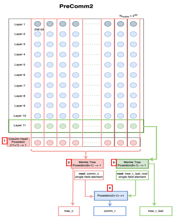
The Filecoin sealing process is composed of four sequential parts: PC1, PC2, C1, and C2. PC1 generates 11 billion elements, each consisting of 32 bytes. The PC2 stage hashes these elements using the Poseidon hash function, grouping 11 elements into a single element. This process is iterated until only one result remains, forming a compact 8-way Merkle tree representation. These hash results are subsequently utilized in the C1 stage. Another, smaller Merkle tree hashes only the 11th element in each group. The two Merkle tree final results are then hashed again and subsequently utilized in the C1 stage.

While the hashing process is essential for data integrity and security, it inherently demands immense computational power and time due to the vast number of elements being processed. Here is where FPGA-based acceleration comes into play.
FPGA-Based Acceleration for PC2
FPGAs are semiconductor devices that can be programmed after manufacturing, enabling users to configure the hardware according to their specific application requirements. FPGAs offer tremendous advantages in parallel processing, making them an ideal choice for accelerating complex computations.
To speed up the PC2 stage in the Filecoin application, we designed a specialized FPGA-based accelerator tailored to the Poseidon hash function. The FPGA’s parallel processing capabilities allowed us to execute multiple hash computations simultaneously. W3BCloud provided reliable and high-speed infrastructure which allowed us to implement, test, and measure performance with their easy-to-use data center resources.
Architecture Overview: Poseidon Processor Ring Topology
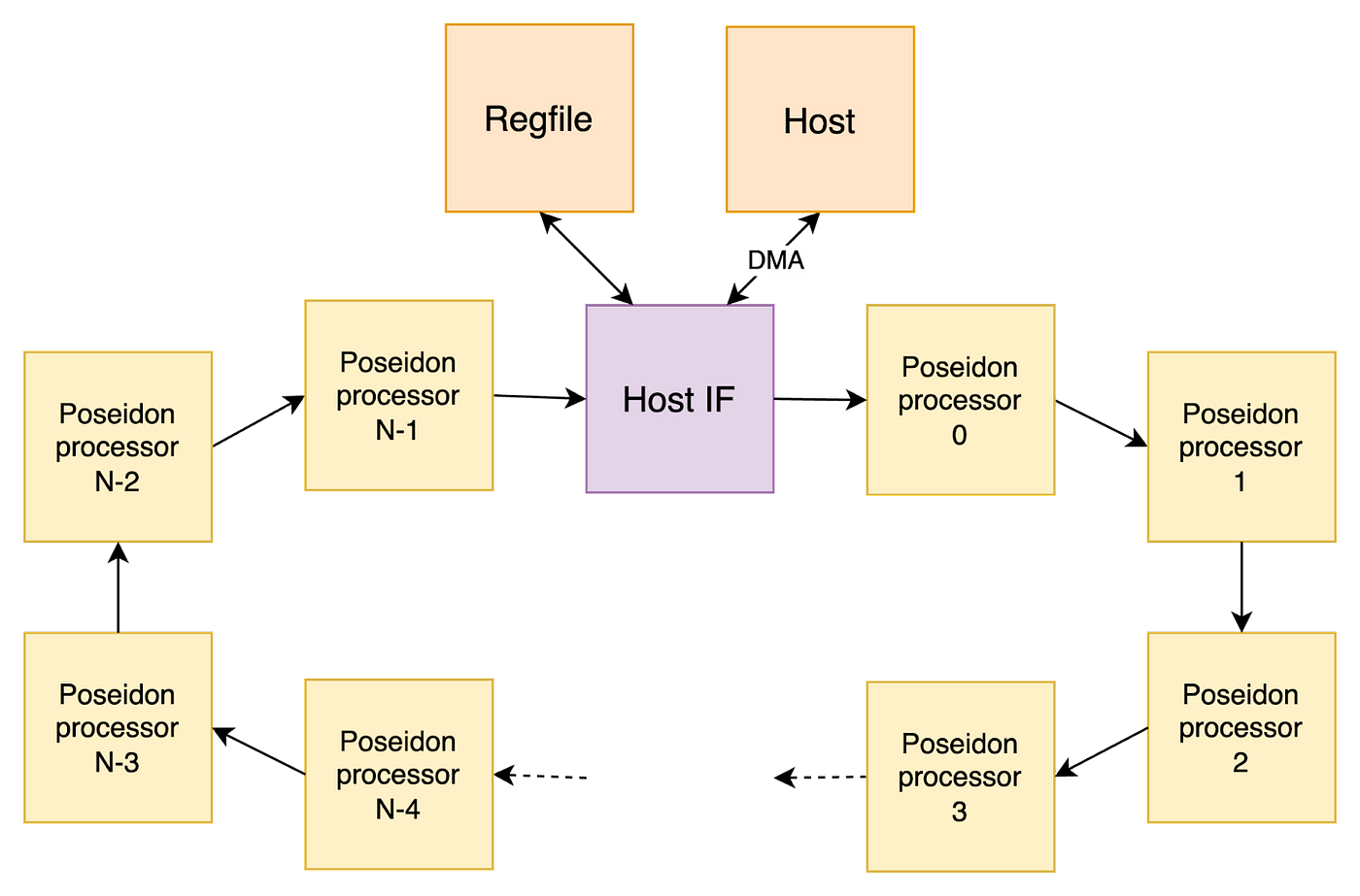
The Poseidon processor ring topology forms the backbone of our FPGA-based accelerator. The topology consists of multiple Poseidon processors, each equipped with dedicated instruction memory, working collaboratively in a directional ring configuration. This topology allows for seamless data flow and efficient data processing.
- Host Interface Node: At the heart of the ring, there is a host interface node responsible for interacting with the host system. This node facilitates bidirectional communication, receiving data through Direct Memory Access (DMA) from the host, and sending it to the Poseidon processors in the ring for processing. Additionally, the host interface collects the hash results generated by the processors and sends them back to the host for further use in the C1 stage of the Filecoin application.
- Ring-Based Communication: The directional ring ensures a continuous flow of data and results between the Poseidon processors. Each processor receives data from its predecessor in the ring and executes a specific program (Poseidon12 or Poseidon9) stored in its instruction memory, depending on the type of data being processed. The result of each computation is then forwarded to the next processor in the ring, forming a chain-like structure that emulates the Merkle tree construction process.
- Thread Management: Each Poseidon processor is capable of managing up to 32 threads simultaneously. These threads operate in parallel on different sets of data, allowing for highly efficient and parallel processing of the input elements. Each thread is assigned a specific functionality, either the Poseidon12 or Poseidon9 hashing program, based on the data being processed.
- Real-time Interaction through Regfile: The host communicates with the Poseidon processors through a register file (regfile). It sends commands to control the ring’s operations, initiates data processing, and manages the threads. Additionally, the regfile provides real-time feedback to the host, reflecting the current status of the network, statistics on processing performance, and helpful debug data for optimization purposes.

Implementation:
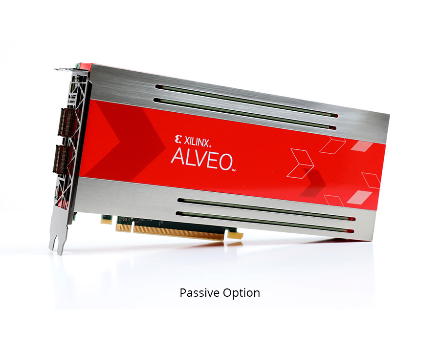
To put our architecture into action, we implemented the FPGA-based Poseidon processor ring topology on Xilinx U250 FPGA card, based on the vu13p FPGA. Our implementation uses 31 Poseidon processors running at clock frequency of 530MHz

The abundant number of processors allowed us to process larger datasets with ease. The U250 FPGA showcased resource utilization, with approximately 75% DSP utilization and around 50% LUT utilization.
Blaze: Empowering FPGA Access and Control
The success of any FPGA-based accelerator lies not only in the efficient hardware implementation but also in the accessibility and ease of use of the software that interfaces with the FPGA. In the case of our PC2 accelerator, we leveraged the power of Blaze, an open-source Rust library, to streamline the integration and control of the FPGA hardware.
Blaze serves as a crucial bridge between the software layer and the FPGA hardware, providing a high-level API that abstracts away the complexities of interacting with FPGAs. Blaze enables developers to seamlessly access and utilize FPGA-based primitives.
Key Features of Blaze:
- Primitives Implementation: Blaze includes pre-built implementations of essential primitives such as MSM, NTT, and the Poseidon hash function.
- Abstraction of FPGA Operations: Blaze simplifies the process of reading and writing data to and from the FPGA, as well as flashing the FPGA with the necessary configurations. By abstracting away these operations, developers can focus on the high-level logic of the application without getting bogged down in low-level FPGA details.
- High-Level API: Blaze offers a high-level API that facilitates easy integration and customization. Developers can utilize a JSON-style configuration setup file to fine-tune the FPGA accelerator’s behavior according to the specific requirements of their application.
- Driver API Support: The Blaze library also provides a comprehensive driver API that covers all the essential methods for FPGA initialization, configuration setting and reading, data transmission to and from the FPGA, as well as loading FPGA images and resetting the FPGA card. This driver API ensures that developers have complete control over the FPGA’s behavior and operations.
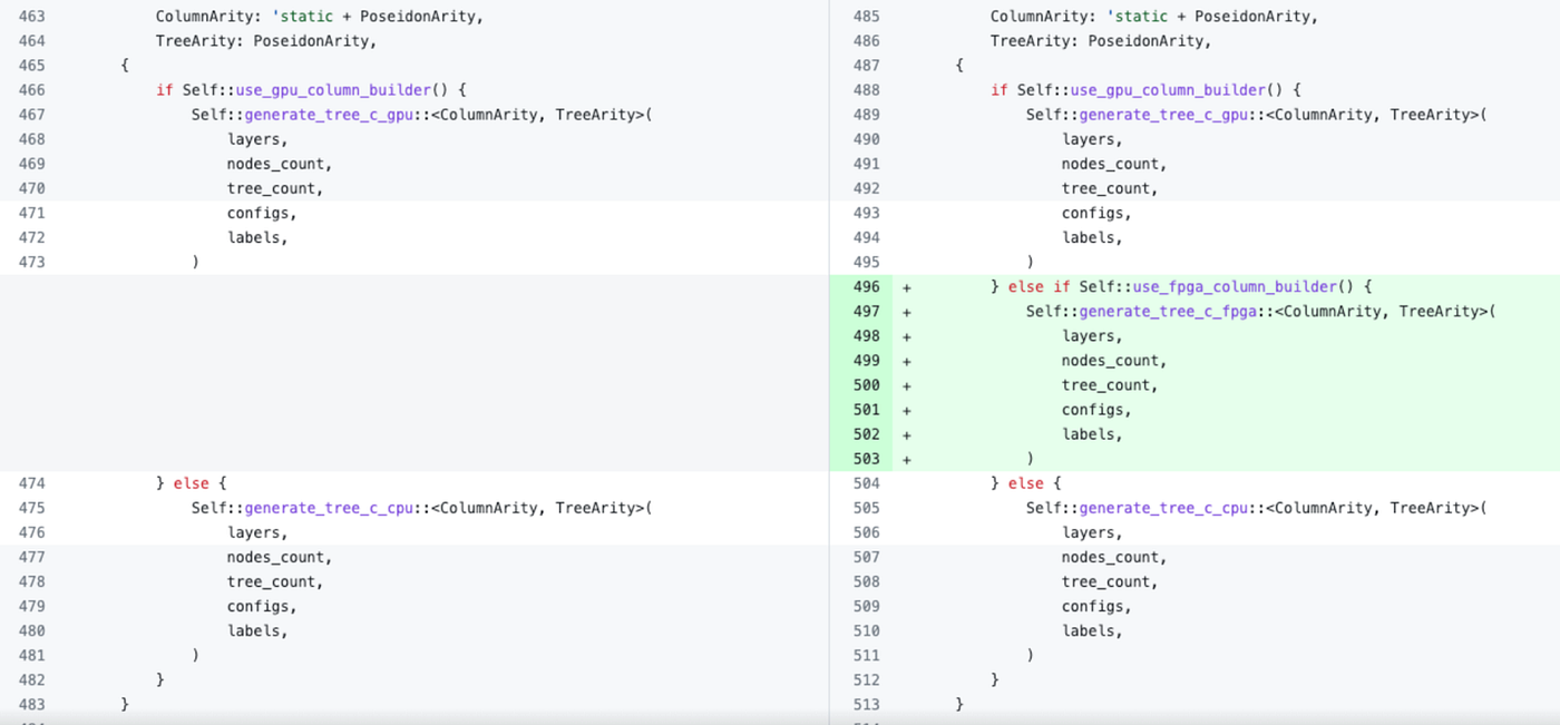
To demonstrate how we use Blaze, here is a code snippet for the changes needed to be done at the original Filecoin Lotus code in order to execute the PC2 Poseidon Merkle tree on the FPGA instead of on CPU:

Performance
Let’s dive into the current performance metrics and the promising future projections.
U250 (vu13p — 16nm technology) Performance Metrics:
- Full PC2 Execution: Currently, with the U250 (vu13p) FPGA running on W3Bcloud infrastructure, the PC2 stage takes approximately 5 minutes and 12 seconds to complete.
- Power Consumption: During PC2 execution, the U250 FPGA consumes 192W of power. The FPGA’s power-efficient design ensures Filecoin sealing can achieve high processing speeds without exorbitant energy demands, making it a more sustainable and environmentally friendly solution.
- Average Temperature: The average operating temperature of the U250 FPGA during PC2 execution remains at a stable and manageable 63°C. This temperature range indicates effective thermal management, ensuring reliable and consistent performance without overheating concerns.
- Short term optimization: host<>card interaction currently has some unnecessary dead times contributing to approximately 30% overhead in PC2 execution time.. Once addressed, we anticipate a significant reduction in PC2 execution time to approximately 4 minutes.
VP1502 (Versal series — 7nm) Projections:
The experimental phase with the VP1502 (Versal series — 7nm) FPGA has already shown promising results, suggesting significant performance improvements in the near future:
- Higher Clock Frequency: The VP1502 FPGA currently achieves an impressive clock frequency of 625MHz with unoptimized code. However, we are confident that further optimizations will allow us to reach a projected clock frequency of 700MHz. This higher clock frequency enhances the overall processing speed, accelerating the PC2 stage even further.
- Increased Processor Count: The VP1502 FPGA supports more processors than its predecessors, allowing for greater parallelism and computational power.
- Reduced Power Consumption: The Versal series FPGA leverages advanced 7nm technology, resulting in reduced power consumption compared to previous generations.
Projected PC2 Execution Time: With these advancements, we expect the PC2 stage’s execution time to be below 3 minutes with additional reduction in power consumption. This solution is therefore expected to be competitive in performance with the latest release of supra_seal GPU implementation which measures 2 minutes and 50 seconds on a 4nm technology (latest generation) GPU.
Departing Thoughts
It is important to decentralize the reliance on a single hardware vendor. What if Nvidia decides that they don’t want to sell GPUs for mining purposes (happened before)? What if, because of demand from AI, we are left with no available GPUs to meet the growing demand of the Filecoin network? We see value in creating diversity for Filecoin mining hardware, adding to the overall resilience of the network against a single hardware provider.
Acknowledgements: Special thanks to Jon Stevens and Swati Gupta for their contributions.
.png)


